Overview
- Doping is a technique used to vary the number of electrons and holes in semiconductors.
- Doping creates N-type material when semiconductor materials from group IV are doped with group V atoms. P-type materials are created when semiconductor materials from group IV are doped with group III atoms.
- N-type materials increase the conductivity of a semiconductor by increasing the number of available electrons; P-type materials increase conductivity by increasing the number of holes present.
It is possible to shift the balance of electrons and holes in a silicon crystal lattice by "doping" it with other atoms.
Atoms with one more valence electron than silicon are used to produce "n-type" semiconductor material. These n-type materials are group V elements in the periodic table, and thus their atoms have 5 valence electrons that can form covalent bonds with the 4 valence electrons that silicon atoms have. Because only 4 valence electrons are needed from each atom (silicon and n-type) to form the covalent bonds around the silicon atoms, the extra valence electron present (because n-type materials have 5 valence electrons) when the two atoms bond is free to participate in conduction. Therefore, more electrons are added to the conduction band and hence increases the number of electrons present.
Atoms with one less valence electron result in "p-type" material. These p-type materials are group III elements in the periodic table. Therefore, p-type material has only 3 valence electrons with which to interact with silicon atoms. The net result is a hole, as not enough electrons are present to form the 4 covalent bonds surrounding the atoms. In p-type material, the number of electrons trapped in bonds is higher, thus effectively increasing the number of holes. In doped material, there is always more of one type of carrier than the other and the type of carrier with the higher concentration is called a "majority carrier", while the lower concentration carrier is called a "minority carrier."
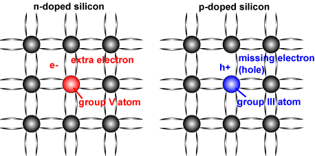
Schematic of a silicon crystal lattice doped with impurities to produce n-type and p-type semiconductor material.
The following table summarizes the properties of semiconductor types in silicon.
| N-type (negative) | P-type (positive) | |
|---|---|---|
| Dopant | Group V (e.g. Phosphorus) | Group III (e.g. Boron) |
| Bonds | Excess Electrons | Missing Electrons (Holes) |
| Majority Carriers | Electrons | Hole |
| Minority Carriers | Holes | Electrons |
The animations below represent p-type and n-type silicon. In a typical semiconductor there might be 1017cm-3 majority carriers and 106cm-3 minority carriers. Expressed in a different form, the ratio of minority to majority carriers is less than one person to the entire population of the planet. Minority carriers are created either thermally or by incident photons.
 N-type semiconductor. These are called "n-type" since the majority carriers are Negatively charged electrons
P-type semiconductor. These are called "p-type" since the majority carriers are Positively charged holes.
- Log in or register to post comments
- 2 comment(s)
 Español
 简体中文
简体中文