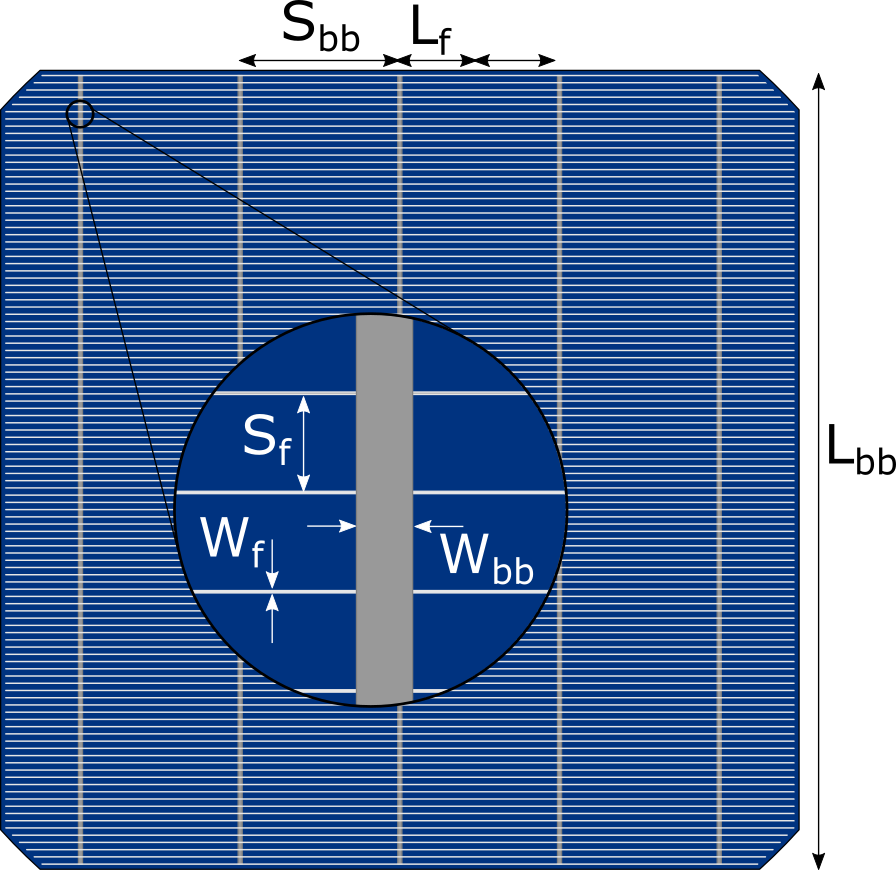
In addition to maximizing absorption and minimizing recombination, the final condition necessary to design a high efficiency solar cell is to minimize parasitic resistive losses. Both shunt and series resistance losses decrease the fill factor and efficiency of a solar cell. A detrimentally low shunt resistance is a processing defect rather than a design parameter. However, the series resistance, controlled by the top contact design and emitter resistance, needs to be carefully designed for each type and size of solar cell structure in order to optimize solar cell efficiency.
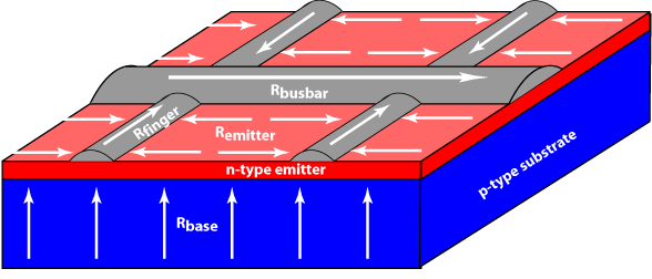
The series resistance of a solar cell consists of several components as shown in the diagram below. Of these components, the emitter and top grid (consisting of the finger and busbar resistance) dominate the overall series resistance and are therefore most heavily optimized in solar cell design.

Resistive components and electron flow in a solar cell.

The power loss in the top contacts is the sum of several components.
Ploss.total = Pfingers + Pemitter + Pcontact + Pbusbars + Pshading.
They are all approximately resistive except for the shading. There are slightly different ways to express the power losses in the top contact grid: either as a power loss or as a series resistance, and both terms can either be total, fractional or per unit area. The results are equivalent but the formulas are slightly different. The following pages use the fractional power loss from each element and the contribution to the series resistance.
