(Coninuation of the previous page. Taken from 1)
At about the same time that selenium cells were under development in the 1930's, silicon was receiving increasing attention for its use in point-contact rectifiers. The rectifying properties of sharpened metal point contacts to various crystals had been known since at least 1874 2. In the early days of radio, such crystal rectifiers were the most commonly used detectors in radio receivers, but with the development of thermionic tubes, crystal rectifiers were replaced in all but ultra-high frequency applications. Tungsten points proved to be the most suitable material for making contact with silicon surfaces. Research into the purity of silicon also led to further understanding of its properties.
In studies of recrystallized melts of pure silicon prepared for this purpose, Ohl 3 discovered the presence of a well-defined barrier in ingots grown from commercially available, high-purity silicon.
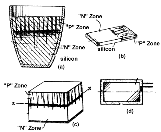
(a) Cast ingot showing natural junction formed by impurity segregation during melting; (b) photovoltaic device cut perpendicular to junction; (c) device cut parallel to junction; (d) top surface of device cut parallel to junction.
In 1941, before even this limited understanding of dopants, silicon photovoltaic devices based on these natural junctions were described 3. In the figure above, (a) shows the naturally grown junction in a cast ingot of silicon. Ingots were produced from acid-leached metallurgical-grade silicon which were cooled from the top after melting. Cells were prepared by cutting from the ingot as indicated in (a). Alternatively, devices could be cut parallel to the junction as shown in (c).
This natural barrier was first found in rods cut from ingots for resistivity measurements. The rods showed good photovoltaic response, were found to have a high thermoelectric coefficient, and had good rectifying properties. One end of the rod developed a negative potential when illuminated or heated and had to be biased negatively in order to show low resistance to current flow across the barrier or across a point contact to this material. Material with these properties became known as negative- or n-type silicon, and material of the opposite type was named positive-, or p-type. Subsequently the role of donor and acceptor impurities in producing these properties was shown.
Although these devices performed similarly to the thin-film devices then available, the preparation method did not obviously lend itself to convenient manufacture. However, it was clear that if a suitable method could be found to activate large areas of silicon surface uniformly, competitive cells could be made. In 1952, improved silicon solar cells were reported by Kingsbury and Ohl 4 using purer silicon to prevent growth junction formation and the ion bombardment of the surface to form the rectifying junction.
Meanwhile, development of crystal growth techniques and techniques for forming junctions by diffusion resulted in the announcement of the first modern silicon cell in 1954 by Chapin, Fuller and Pearson 5. These cells had the dual rear contact structure of the figure below and had an efficiency of 6%, about 15 times that of earlier devices, opening the first real prospects for power generation using photovoltaics. Considerable interest was aroused 6. However, given the immaturity of the silicon preparation industry, it soon became apparent that the initial enthusiasm was premature. Nevertheless, the cells proved suitable for space use and this formed their major application until the early 1970's.
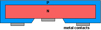
Early silicon solar cell structure.
- 1. , “Photovoltaics: Coming of Age”, 21st IEEE Photovoltaic Specialists Conference. Orlando, USA, pp. 1-8, 1990.
- 2. , “On Conductance in Metal Sulphides”, Ann. d. Physik, vol. 153, p. 556, 1874.
- 3. a. b. , “Light-Sensitive Electric Device”, U.S. Patent, vol. 2, p. 402, 602, 1941.
- 4. , “Photoelectric Properties of Tonically Bombarded Silicon”, Bell Systems Technical Journal, vol. 31, pp. 802-815, 1952.
- 5. , “A New Silicon P-N Junction Photocell for Converting Solar Radiation into Electrical Power”, Journal of Applied Physics, vol. 25, pp. 676-677, 1954.
- 6. “Bell Laboratories Record”. 1955.