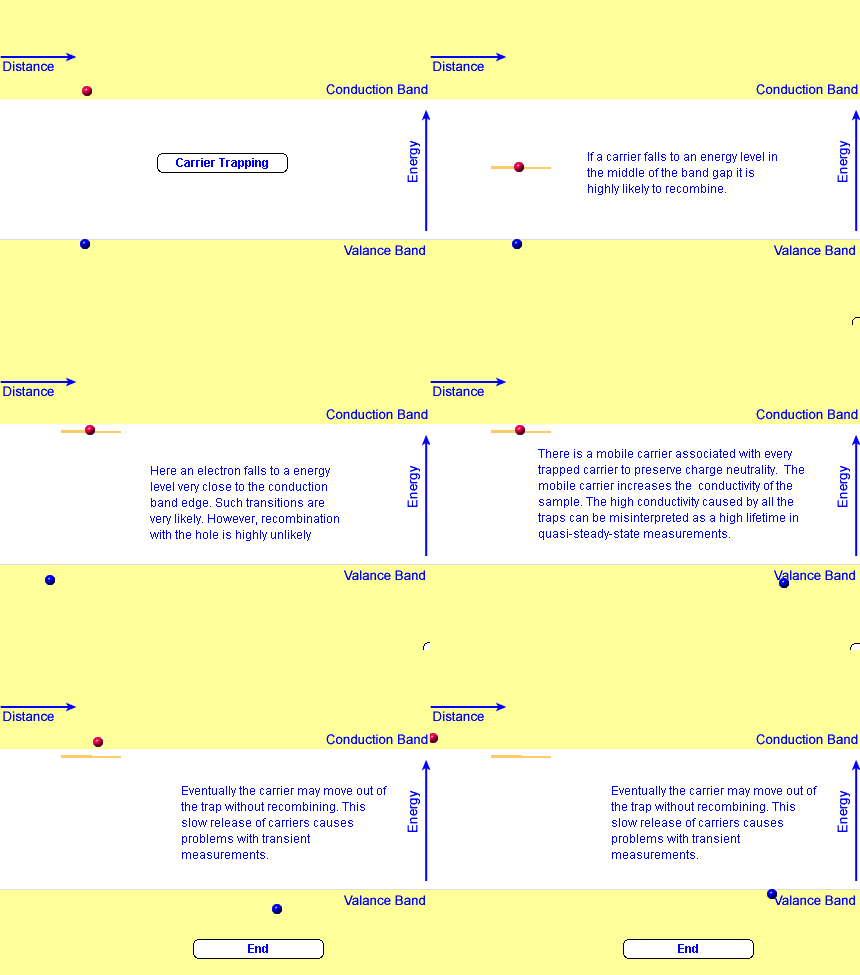
For energy levels created in the middle of the band gap by impurities (deep level "traps"), the probability of capturing electrons and hole is similar, so traps at mid-gap operate as recombination centers. For energy levels near the band edges the probability of capturing one carrier is much higher than the other. For example in the animation below, the probability of capturing electrons is much higher than for capturing holes. Electrons tend to get trapped but they don't recombine, so shallow traps don't reduce the minority carrier lifetime. However, the shallow level traps do cause significant problems with lifetime measurements

The trapped carrier has a mobile carrier of the opposite polarity associated with it to preserve charge neutrality. In the animation, the trapped electron has a mobile hole associated with it that increases the wafer conductivity. Since QSS measurements use the carrier concentration under steady state conditions as a measure of carrier lifetime, the extra carriers are confused with a high lifetime material. The number of shallow traps is usually quite low but the traps fill first, so at very low injection levels the traps dominate the QSS measurements and need to be corrected for. As the number of carriers generated by light increases, the percentage of carriers trapped is only a very small section of the total and so the traps only have a very small effect. Since the number of trapped carriers is roughly constant with injection level, the traps can be corrected for.
For transient measurements, the slow release of carriers out of the traps that causes problems.
Correcting for the Effect of Traps
The presence of traps causes spuriously large lifetimes at low injection levels. The use of a bias light saturates the traps enabling the measurement of the lifetime. In QSS measurements the bias light can either be an external source of infrared light (Ref) or part of the same light used for the lifetime measurement 1. The level of bias light is adjusted to that it just saturates the traps 2.
- 1. , «Contactless determination of current–voltage characteristics and minority-carrier lifetimes in semiconductors from quasi-steady-state photoconductance data», Applied Physics Letters, vol. 69, pp. 2510-2512, 1996.
- 2. , «On the use of a bias-light correction for trapping effects in photoconductance-based lifetime measurements of silicon», Journal of Applied Physics, vol. 89, pp. 2772-2778, 2001.
