SEM
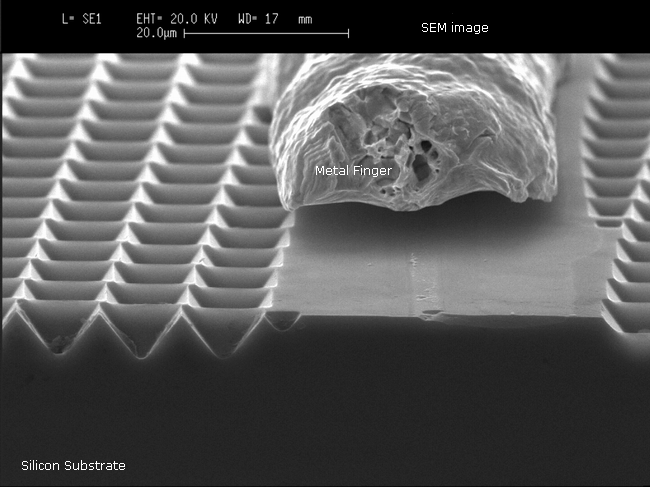
Scanning electron microscope (SEM) pictures are useful for examining the fine structure of solar cells. Even in large area commercial devices, for example, an SEM photograph can show the depth of the rear surface aluminium alloyed layer. Many of the cell features are of the order of microns and so not possible to view with an optical microscope. An additional advantage of an electron microscope is its higher depth of field. With an electron microscope it is possible to have the whole device in focus at once whereas in an optical microscope at high magnification only parts of the device will be in focus at any time.
EBIC
Electron Beam induced current (EBIC) is useful for showing the electrically active areas of the device. To create an EBIC image an electron beam is swept across the sample and the output current of the device measured. Those electrons that are collected by the junction show up as bright regions while electrons uncollected remain dark. It is common to superimpose the EBIC images on SEM picture to show more clearly show the location of the active areas.
In the figure below the cell has been cleaved to take a picture of the cell edge. The cleaved surface is unpassivated so most carriers will recombine in a very short distance and only those created right at the junction edge will be collected. Hence the junction shows up as a very bright line.
EBIC is also used in material characterisation. Altering the energy of the beam changes the depth and volume at of electrical excitation and this can be used to characterise defects. By sweeping the beam across the surface of the device it is possible to identify the electrically inactive areas such as grain boundaries. A numerical analysis of the induced current gives a measure of the diffusion length 1.
SEM picture of a cleaved PERL solar cell. Click on the image to change to an EBIC view. In the EBIC view the brightest area is around the junction between the n-type diffusion and the p-type base. It shows that the emitter diffusion is quite shallow at 1-2 µm and that it follows the surface topology. It also shows that the diffusion under the finger contact is 15 µm wide and 3 µm deep. (Photo: Tom Puzzer)

EBIC image superimposed on an SEM image of an aluminium alloyed rear surface layer. Such layers are typically used as back-surface-fields in commercial solar cells. The bright line of the silicon-aluminium juction shows that the aluminium layer is highly non-uniform. Optimisation of the processing conditions led to much more uniform layers 2, 3.
- 1. , «Simulating Electron-Beam-Induced Current Profiles Across p-n Junctions», 16h European Solar Energy Conference. с. 1590-1593, 2000.
- 2. , «Dependence of aluminium alloying on solar cell processing conditions», 13th Workshop on Crystalline Silicon Solar Cell Materials and Processes. 2003.
- 3. , «Aluminium Back Surface Field in Buried Contact Solar Cells», University of New South Wales, 2000.

