Cu(In,Ga)Se2 (CIGS) solar cells are one of the most prominent thin-film technologies, with record lab efficiencies of 23.4% achieved in 20191 by Solar Frontier2 3. The CIGS material has a direct bandgap and high absorption coefficient. Efficient sunlight absorption can be achieved in CIGS layers as thin as 1 µm, 100 times thinner than a crystalline silicon solar cell4, as evidenced in Figure 1. This gives promise to the potential of high efficiency solar cells made with minimal material consumption. Another major characteristic of this material is that beneficial optoelectronic properties can be obtained with a wide range of compositional variations. In addition, CIGS material made by alloying CuInSe2 with varying Ga concentrations allows for tuning of the bandgap. High-efficiency CuIn1-xGaxSe2 devices often have a Ga content of x≈3.5 Additional elements such as Ag or S can be added to the alloy to increase the bandgap.

The CIGS family of solar cells evolved from CuInSe2 ternary alloy solar cells .6 The first CuInSe2 solar cells were developed in 1974 at Bell Laboratories.7 These cells were grown using single crystals and achieved power conversion efficiencies of 12%. Subsequent improvements would enable a polycrystalline thin-film design. The first commercial CIGS cells were sold by Arco Solar in 1988.8
The active CIGS layer is a polycrystalline film with the chalcopyrite crystal structure. The CIGS absorber layer is a p-type material in contact with an n-type CdS layer. Control of the concentration of copper in the film allows for the creation of a copper deficient phase near the CdS interface referred to as an Ordered Defect Compound (ODC). The ODC passivates the surface, therefore reducing interface recombination at the CIGS/CdS junction.
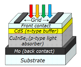
The most common CIGS structure is grown on soda-lime glass, and an example is shown in Figure 2. A molybdenum layer is sputtered on top of the glass to form the back contact. It has been found that sodium from the glass diffuses through the Mo layer and into the CIGS layer.9 The role of Na on improving the device performance is not fully understood but it has been associated with passivation of surface grain boundary defects and increased charge carrier concentration.10 CIGS can be grown on a variety of substrates besides soda-lime glass, however growth on metal or flexible plastic substrates requires the addition of external sodium.11 A p-type CIGS layer is deposited, acting as the photoactive layer. A n-type buffer layer is then grown on top of the CIGS layer, typically CdS deposited by chemical bath deposition. Front contacts are usually provided with a ZnO window layer and an Al-doped ZnO transparent conducting oxide layer. The device is finished by depositing metal grids for improved current collection.
Many techniques have been attempted for the growth of CIGS films: sputtering, evaporation, electrochemical deposition, nanoparticle printing, and ion-beam deposition.6 The most common processes are referred to as selenization and co-evaporation. The selenization process occurs in two parts by preparing a Cu-In-Ga metal precursor in the first step, followed by a reaction in a Se and/or S atmosphere in the second step to form the CIGS film. Co-evaporation is a physical vapor deposition technique involving simultaneous evaporation of Cu, In, Ga, and Se in a vacuum chamber. For years the world record efficiencies for CIGS were obtained by the co-evaporation method; however, in early 2014, Solar Frontier achieved a 20.9% conversion efficiency from a CIGS cell produced using the selenization method.3 Since then, there has been a close competition on the world record efficiencies between these two processes.
CIGS still faces several challenges in order to compete with other photovoltaics. For example, the role that Ga composition gradients and sodium concentration has on device performance is not completely understood. Also, increasing the Ga content allows progress toward CIGS solar cells with potentially higher cell efficiencies; however, achieving improved efficiency for high Ga compositions is still a challenge. Increased insight on recombination and defects in CIGS would also lead to improved electrical performance. There is also a significant difference between laboratory solar cells versus large-scale modules.12 One issue at the module level is choosing a proper TCO with adequate thickness but with reduced free carrier absorption.12
Since CIGS cells are a thin-film technology, they enable different panel configurations than might be achieved with crystalline silicon solar cells. In monolithically interconnected (MLI) panels, devices are grown on a single glass substrate and are connected in series using a laser scribe.6 This eliminates the need for many of the solder points and diodes which can be common points of failure in crystalline Si or cell-cased CIGS.
Acknowledgement
The material on this page was developed as part of the 2016 Hands-On PV Experience (HOPE) Workshop at NREL.
Contributing authors: Jimmy Hack, Kevin Jones, Sina Soltanmohammad, Nicholas Valdes
Department of Materials Science and Engineering, University of Delaware
- 1. , “Cd-Free Cu(In,Ga)(Se,S)2 Thin-Film Solar Cell With Record Efficiency of 23.35%”, IEEE Journal of Photovoltaics, vol. 9, pp. 1863-1867, 2019.
- 2. , “Effects of heavy alkali elements in Cu (In, Ga) Se2 solar cells with efficiencies up to 22.6%”, physica status solidi (RRL)–Rapid Research Letters, vol. 10, pp. 583–586, 2016.
- 3. a. b. , “Recent R&D progress in solar frontier's small-sized Cu (InGa)(SeS)2 solar cells”, in 2014 IEEE 40th Photovoltaic Specialist Conference (PVSC), 2014.
- 4. , “The Influence of Absorber Thickness on Cu(In,Ga)Se2 Solar Cells With Different Buffer Layers”, IEEE journal of photovoltaics, vol. 3, pp. 1376–1382, 2013.
- 5. , “High-efficiency Cu(In,Ga)Se2 cells and modules”, Solar energy materials and solar cells, vol. 119, pp. 51–58, 2013.
- 6. a. b. c. d. , “Cu(InGa)Se2 Solar Cells”, in Handbook of photovoltaic science and engineering, 2nd ed., John Wiley & Sons, 2011, pp. 546-599.
- 7. , “CuInSe2/CdS heterojunction photovoltaic detectors”, Applied Physics Letters, vol. 25, pp. 434–435, 1974.
- 8. , “Cu(In,Ga)Se2 Thin-Film Solar Cells”, in Solar Cells: Materials, Manufacture and Operation, London: Academic Press, 2012, p. 262.
- 9. , “Na incorporation in Mo and CuInSe2 from production processes”, Solar energy materials and solar cells, vol. 59, pp. 255–264, 1999.
- 10. , “Effects of Na on the electrical and structural properties of CuInSe2”, Journal of Applied Physics, vol. 85, pp. 7214–7218, 1999.
- 11. , “Effects of NaF coevaporation on structural properties of Cu (In, Ga) Se2 thin films”, Thin Solid Films, vol. 431, pp. 37–40, 2003.
- 12. a. b. , “Progress in thin film CIGS photovoltaics–Research and development, manufacturing, and applications”, Progress in Photovoltaics: Research and Applications, vol. 25, pp. 645–667, 2017.