(Taken from Green1 which makes use of Benjamin2, Shive3 and Wolf4)
Edmond Becquerel appears to have been the first to demonstrate the photovoltaic effect5 6. Working in his father's laboratory as a nineteen year old, he generated electricity by illuminating an electrode with different types of light, including sunlight (see the figure below). Best results were obtained with blue or ultraviolet light and when electrodes were coated with light sensitive material such as AgCl or AgBr. Although he usually used platinum electrodes, he also observed some response with silver electrodes. He subsequently found a use for the photovoltaic effect by developing an "actinograph" which was used to record the temperature of heated bodies by measuring the emitted light intensity.
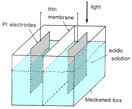
Diagram of apparatus described by Becquerel (1839)
The next significant photovoltaic development arose from the interest in the photoconductive effect in selenium. While investigating this effect, Adams and Day (1877)7 noted an anomaly they thought could be explained by the generation of internal voltages. They investigated this anomaly more carefully using samples as shown below. Heated platinum contacts were pushed into opposite ends of small cylinders of vitreous selenium. The objective of one experiment conducted by Adams and Day upon such specimens was to see 'whether it would be possible to start a current in the selenium merely by the action of light'.

Sample geometry used by Adams and Day (1876) for the investigation of the photoelectric effects in selenium.
The result was positive! This was the first demonstration of the photovoltaic effect in an all solid-state system. Adams and Day attributed the photogenerated currents to light induced crystallization of the outer layers of the selenium bar. Several decades were to pass before the development of physics allowed more insight into this process.
The next significant step forward came seven years later with the work of Fritts (1883) 8. By compressing molten selenium between plates made from two different metals, Fritts was able to prepare thin Se films which adhered to one of the two plates, but not to the other. By pressing a gold leaf to the exposed selenium surface, he thereby prepared the first "thin-film" photovoltaic devices. These first thin-film devices were as large as 30 cm2 in area.
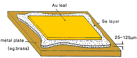
Thin-film selenium demonstrated by Fritts in 1883.
He was also the first to recognize the enormous potential of photovoltaic devices. He saw that the devices could be fabricated at very low cost and noted that 'the current, if not wanted immediately, can either be "stored" where produced, in storage batteries … or transmitted … to a distance, and there used, or stored'.
It was, however, to be nearly fifty years before there was another significant burst of activity in this area.
While studying photoconductive effects in cuprous oxide layers grown on copper, the rectifying action of the copper-cuprous oxide junction was discovered. This led to the development of large-area rectifiers, followed soon after by large-area photocells. Grondahl 9 describes the development of both copper-cuprous oxide rectifiers and photovoltaic cells.
The figure below shows the very simple structure used by the earlier cells based on the copper-cuprous oxide junction. A coil of Pb wire is used to give a grid contact to the illuminated surface of the cell. This approach was subsequently refined by sputtering the metal on the outer surface and removing a part of it so as 'to form a grid of any desired fineness'. These developments seem to have stimulated a great deal of activity in this area. Grondahl 9 documents 38 publications dealing with copper-cuprous oxide photovoltaic cells over the period 1930-32. 10
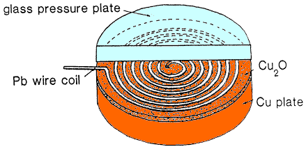
Early Grondahl-Geiger copper-cuprous oxide photovoltaic cell (circa 1927).
This activity also seems to have reawakened interest in selenium as a photovoltaic material. In particular, Bergmann 11 reported improved selenium devices in 1931. These proved superior to the copper-based devices and became the commercially dominant product. In 1939, a thallous-sulphide cell of similar performance was also reported by Nix 10. The structure of this device and of the most efficient selenium and copper-cuprous oxide devices took the form shown in the figure below.
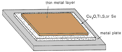
Structure of the most efficient photovoltaic devices developed during the 1930's.
- 1. , «Photovoltaics: Coming of Age», 21st IEEE Photovoltaic Specialists Conference. Orlando, USA, pp. 1-8, 1990.
- 2. , «Voltaic Cell, Chapter XIV», New York: Wiley, 1983.
- 3. , «Semiconductor Devices, Chapter 8», New Jersey: Van Nostrand, 1959.
- 4. , «Historical Development of Solar Cells». IEEE Press, 1976.
- 5. , «Recherches sur les effets de la radiation chimique de la lumiere solaire au moyen des courants electriques», Comptes Rendus de L´Academie des Sciences, vol. 9, pp. 145-149, 1839.
- 6. , «Memoire sur les effects d´electriques produits sous l´influence des rayons solaires», Annalen der Physick und Chemie, vol. 54, pp. 35-42, 1841.
- 7. , «The Action of Light on Selenium», Proceedings of the Royal Society, London, vol. A25, p. 113, 1877.
- 8. , «On a New Form of Selenium Photocell», American J. of Science, vol. 26, p. 465, 1883.
- 9. a. b. , «The Copper-Cuprous-Oxide Rectifier and Photoelectric Cell», Review of Modern Physics, vol. 5, p. 141, 1933.
- 10. a. b. , «A Thallous Sulphide Photo EMF Cell», Journal Opt. Society of America, vol. 29, p. 457, 1939.
- 11. , «Uber eine neue Selen- Sperrschicht Photozelle», Physikalische Zeitschrift, vol. 32, p. 286, 1931.