Techniques for the production of multicrystalline silicon are simpler, and therefore cheaper, than those required for single crystal material. However, the material quality of multicrystalline material is lower than that of single crystalline material due to the presence of grain boundaries. Grain boundaries introduce high localized regions of recombination due to the introduction of extra defect energy levels into the band gap, thus reducing the overall minority carrier lifetime from the material. In addition, grain boundaries reduce solar cell performance by blocking carrier flows and providing shunting paths for current flow across the p-n junction.
It used to be thought that large grain crystals were the most suitable for multicrystalline silicon solar cells since larger crystals meant fewer grain boundaries. However, in recent years it was found that smaller grains gave lower stress at the ground boundaries so they were less electrically active (lower recombination). Presently, most multicystalline silicon for solar cells is grown using a process where the growth is seeded to produce smaller grains and referred to as "high performance multi"1

Slab of multicrystalline silicon after growth. The slab is further cut up into bricks and then the bricks are sliced into wafers.
To avoid significant recombination losses at grain boundaries, grain sizes on the order of at least a few millimeters are required 2. This also allows single grains to extend from front to back of the cell, providing less resistance to carrier flow and generally decreasing the length of grain boundaries per unit of cell. Such multicrystalline material is widely used for commercial solar cell production.

At the boundary between two crystal grains, the bonds are strained, degrading the electronic properties.
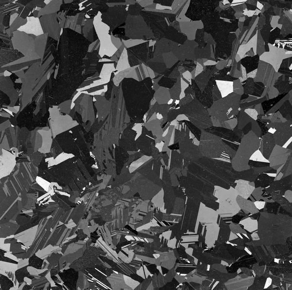
A 10 x 10 cm2 multicrystalline wafer. The wafer has been textured so that grains of different orientation show up as light and dark.
Although more than half of the manufactured modules used multicrystalline silicon for many years, starting in 2018, monocrystalline silicon began to dominate and by 2020 and 2021 it became difficult to buy multicyrstalline silicon cells. The reasons for the change were complex, but were aligned with a transition from using aluminum-back-surface-field cell designs to using passivated-emitter rear contact (PERC) structures. Although high efficiencies were achieved with PERC cells as early as 1990, these did not become commercially viable before about 2015. The PERC structure enables higher efficiencies for monocrystalline cells, but does not give much performance boost for multicrystalline cells. Additionally, the introduction of "cast-mono" has blurred the difference between mono- and multicrystalline silicon. See, for example, https://www.youtube.com/watch?v=EZQtJU0Ib9Q.
- 1. «Development of high-performance multicrystalline silicon for photovoltaic industry», Progress in Photovoltaics: Research and Applications, vol. 23, n.º 3, pp. 340 - 351, 2015.
- 2. , «Electronic processes at grain boundaries in polycrystalline semiconductors under optical illumination», IEEE Transactions on Electron Devices, vol. ED-24, pp. 397-402, 1977.
- Log in or register to post comments
- 1 comment(s)
 Español